Detailed architecture
MeluXina CPUs
The following table will give you insight into MeluXina compute Modules' microprocessors architecture. To get the best possible performance out of each system, of particular interest will be the cache sizes and NUMA node allocations per type of compute node. NUMA is further described in the following sections.
| Characteristics | Cluster node | Accel. (GPU) node | Accel. (FPGA) node | Large Memory node |
|---|---|---|---|---|
| Architecture | x86_64 | x86_64 | x86_64 | x86_64 |
| CPU op-mode(s) | 32-bit, 64-bit | 32-bit, 64-bit | 32-bit, 64-bit | 32-bit, 64-bit |
| Byte Order | Little Endian | Little Endian | Little Endian | Little Endian |
| CPU logical cores/node | 256 | 128 | 128 | 256 |
| Thread(s) per core | 2 | 2 | 2 | 2 |
| Core(s) per socket | 64 | 32 | 32 | 64 |
| Socket(s) | 2 | 2 | 2 | 2 |
| NUMA node(s) | 8 | 4 | 8 | 8 |
| Model name | AMD EPYC 7H12 64-Core Processor | AMD EPYC 7452 32-Core Processor | AMD EPYC 7452 32-Core Processor | AMD EPYC 7H12 64-Core Processor |
| CPU base MHz | 2600 | 2350 | 2350 | 2600 |
| L1d cache | 32K | 32K | 32K | 32K |
| L1i cache | 32K | 32K | 32K | 32K |
| L2 cache | 512K | 512K | 512K | 512K |
| L3 cache | 16384K | 16384K | 16384K | 16384K |
| NUMA node0 CPU(s) | 0-15,128-143 | 0-15,64-79 | 0-7,64-71 | 0-15,128-143 |
| NUMA node1 CPU(s) | 16-31,144-159 | 16-31,80-95 | 8-15,72-79 | 16-31,144-159 |
| NUMA node2 CPU(s) | 32-47,160-175 | 32-47,96-111 | 16-23,80-87 | 32-47,160-175 |
| NUMA node3 CPU(s) | 48-63,176-191 | 48-63,112-127 | 24-31,88-95 | 48-63,176-191 |
| NUMA node4 CPU(s) | 64-79,192-207 | - | 32-39,96-103 | 64-79,192-207 |
| NUMA node5 CPU(s) | 80-95,208-223 | - | 40-47,104-111 | 80-95,208-223 |
| NUMA node6 CPU(s) | 96-111,224-239 | - | 48-55,112-119 | 96-111,224-239 |
| NUMA node7 CPU(s) | 112-127,240-255 | - | 56-63,120-127 | 112-127,240-255 |
NUMA architecture
NUMA stands for Non-Uniform Memory Access and is a shared memory architecture used in multiprocessing systems. A specific local memory is attached to each CPU but can access memory from any other CPUs in the system. In this way, each CPU can access its local memory much faster than a remote memory, with lower latency and higher bandwidth performance.
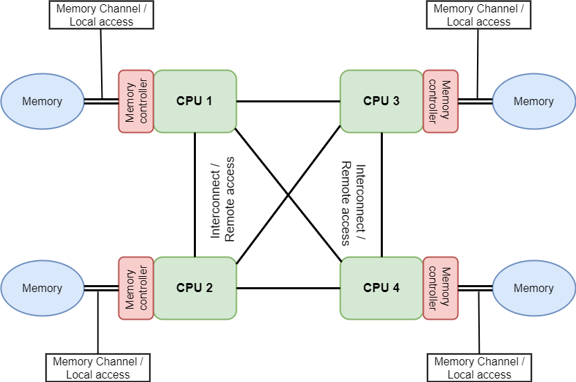
Representation of a 4 CPUs NUMA node architecture.
In order to take advantage of the NUMA architecture and for optimizing CPU accesses, users should attempt to:
- allocate most or all of a task's memory to one CPU's local RAM.
- schedule a task to the CPU/core directly connected to the majority of that task's memory.
Check out the manual of the numactl tool for more details on how to apply these optimizations when running your applications.
AMD EPYC
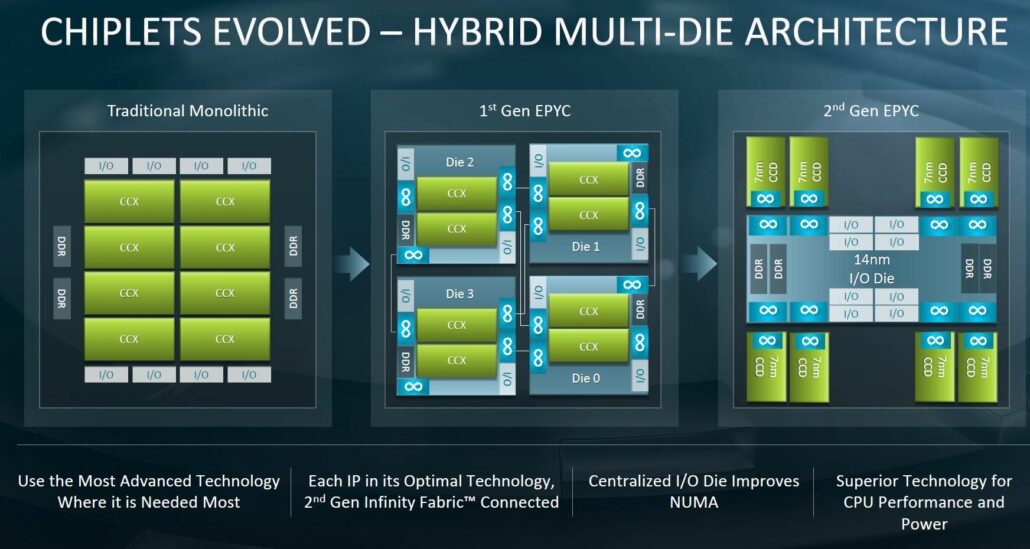
MeluXina CPU and Large Memory nodes include EPYC 7H12-AMD CPUs which is a 64-bit 64-core x86 server microprocessor based on the Zen 2 micro-architecture. It is divided into 4 quadrants, with up to 2 Core Complex Dies (CCDs) per quadrant. Each CCD consists of two Core CompleXes (CCX). Each iCCX has 4 cores that share an L3 cache. All 4 CCDs communicate via 1 central die for IO called I/O Die (IOD).
In multi-chip processors such as the AMD-EPYC series, differing distances between a CPU core and the memory can cause Non-Uniform Memory Access (NUMA) issues. AMD offers a variety of settings to help limit the impact of NUMA. One of the key options is called Nodes per Socket (NPS). There are 8 memory controllers per socket that support eight memory channels running DDR4, supporting up to 2 DIMMs per channel.
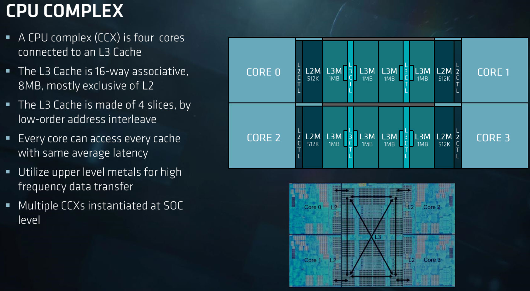
AMD ROME Core and memory architecture (Source here)
With this architecture, all cores on a single CCD are closest to 2 memory channels. The rest of the memory channels are across the IO die, at differing distances from these cores. Memory interleaving allows a CPU to efficiently spread memory accesses across multiple DIMMs. This allows more memory accesses to execute without waiting for one to complete, maximizing performance. Memory interleaving is achieved by using NUMA in Nodes Per Socket (NPS).
MeluXina CPUs use the NPS4 workload type for CPU, FPGA, and Large Memory compute nodes. NPS4 configuration partitions the CPU into four NUMA domains. Each quadrant is a NUMA domain, and memory is interleaved across the 2 memory channels in each quadrant. PCIe device's will be local to one of the 4 NUMA domains on the socket, depending on the quadrant of the IOD that has the PCIe root for the device.
A detailed topology view is provided by the hwloc (Hardware Locality) tool which aims at easing the process of discovering hardware resources in parallel architectures. It offers a detailed representation of the resources, their locality, attributes and interconnection.
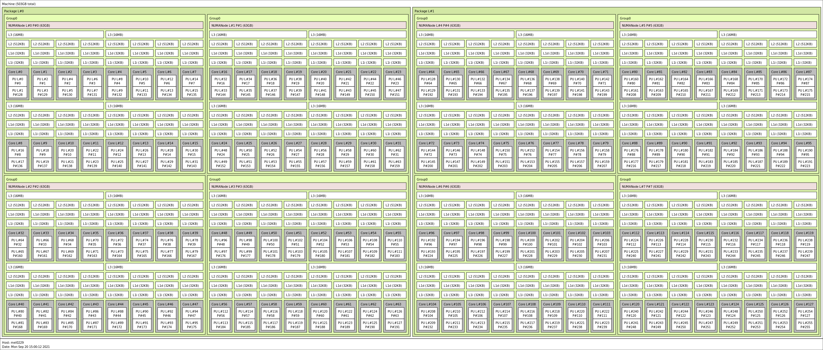 A detailed NUMA architecture of a CPU node on MeluXina (Click on image to expand it).
MeluXina NVIDIA A100 GPUs
The 200 Accelerator Module GPU nodes are based on the NVIDIA A100 GPU-AI accelerators. Each GPU has 40GB of on-board High Bandwidth Memory and the 4 GPUs on each compute node are linked together with the NVLink 3 interconnect (1,555GB/s memory bandwidth). The A100 supports the Multi-Instance GPU feature, allowing the GPUs to be split up into 7 'independent' with 5 GB each.
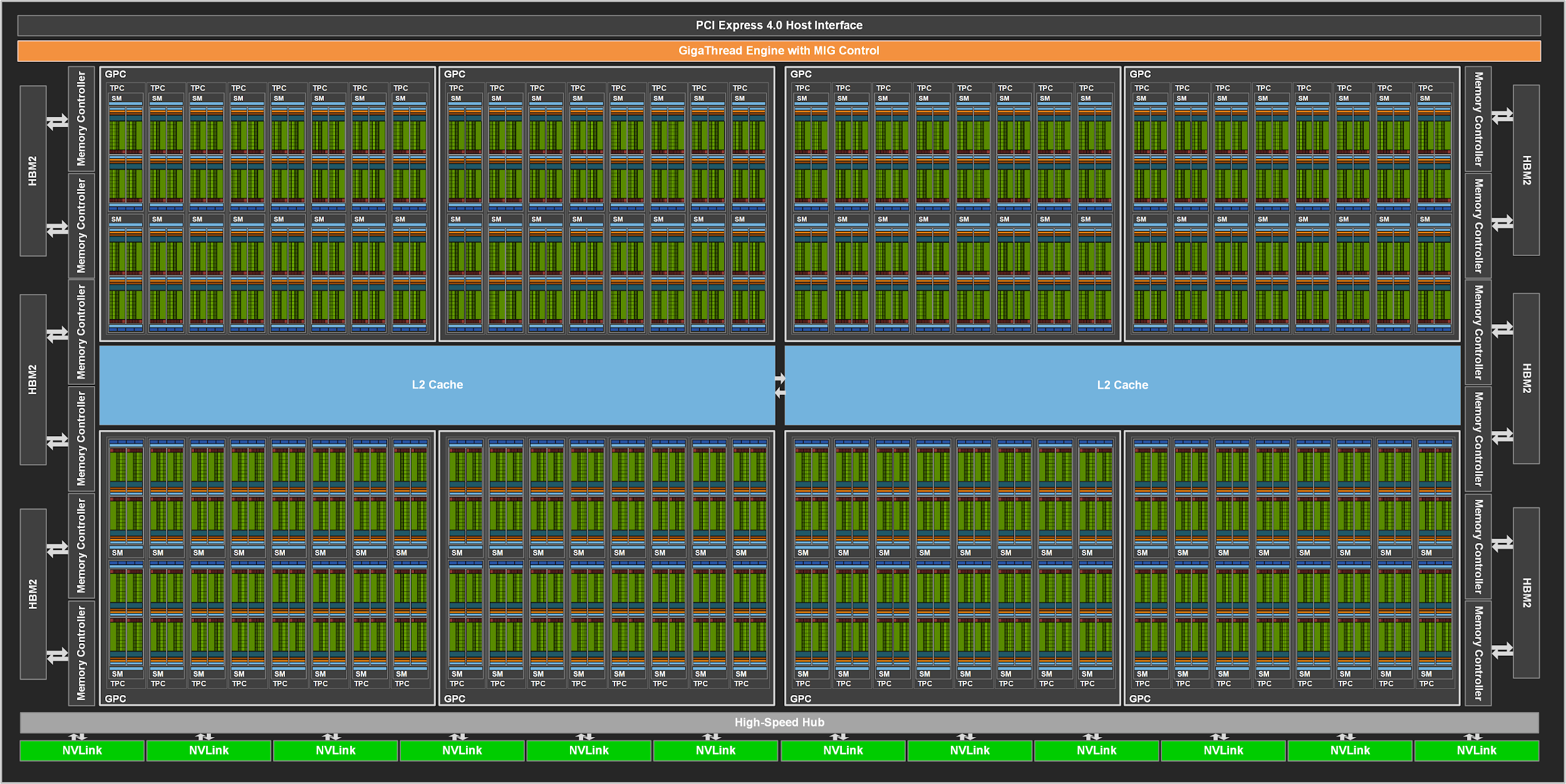
This picture describes a GA100 Full GPU with 128 SMs.
However, on Meluxina, the A100 Tensor Core GPU is slightly different and consists of an 108 SMs based implementation. (click on image to expand it).
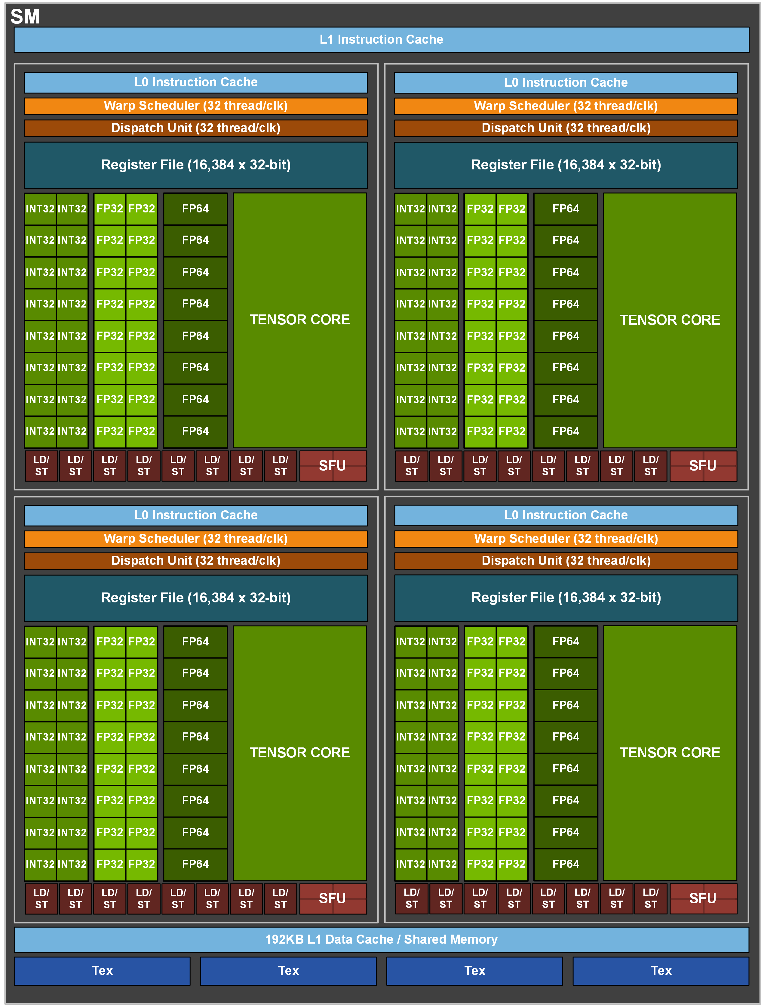
GA100 SM (click on image to expand it).
The A100 with 108 SMs provides higher performance and new features compared to the previous Volta and Turing generations. Key SM features are briefly highlighted below, check out the Ampere architecture white paper for additional details. NVIDIA also provides a dedicated tuning guide for the Ampere-based GPUs, enabling developers to take advantage of the new features.
- Third-generation Tensor Cores:
- Acceleration for all data types including FP16, BF16, TF32, FP64, INT8, INT4, and Binary.
- New Tensor Core sparsity feature exploits fine-grained structured sparsity in deep learning networks, doubling the performance of standard Tensor Core operations. NVIDIA A100 Tensor Core GPU Architecture In-Depth 21 NVIDIA A100 Tensor Core GPU Architecture
- TF32 Tensor Core operations in A100 provide an easy path to accelerate FP32 input/output data in DL frameworks and HPC, running 10x faster than V100 FP32 FMA operations, or 20x faster with sparsity.
- FP16/FP32 mixed-precision Tensor Core operations deliver unprecedented processing power for DL, running 2.5x faster than Tesla V100 Tensor Core operations, increasing to 5x with sparsity.
- BF16/FP32 mixed-precision Tensor Core operations run at the same rate as FP16/FP32 mixed-precision.
- FP64 Tensor Core operations deliver unprecedented double precision processing power for HPC, running 2.5x faster than V100 FP64 DFMA operations.
- INT8 Tensor Core operations with sparsity deliver unprecedented processing power for DL Inference, running up to 20x faster than V100 INT8 operations.
- 192 KB of combined shared memory and L1 data cache, 1.5x larger than V100 SM
- New asynchronous copy instruction loads data directly from global memory into shared memory, optionally bypassing L1 cache, and eliminating the need for intermediate register file (RF) usage
- New shared-memory-based barrier unit (asynchronous barriers) for use with the new asynchronous copy instruction
- New instructions for L2 cache management and residency controls
- New warp-level reduction instructions supported by CUDA Cooperative Groups
- Many programmability improvements which reduce software complexity
Note that the full GA-100 and the A100 implementations each includes (see Ampere architecture white paper, p.19):
- 4 Third-generation Tensor Cores per SM
- 64 Int/FP32 Cuda Cores per SM (6912 Int/FP32 cores per A-100 GPU)
- 32 FP64 Cuda Cores per SM (3456 FP64 cores per A-100 GPU)
For more resources on how to program and develop your code on the A100 GPUs and NVIDIA GPUs in general, see the CUDA programming language and PGI compiler, NVIDIA HPC SDK (A Comprehensive Suite of Compilers, Libraries, and Tools for HPC) materials available from NVIDIA.
MeluXina Bittware 520N-MX FPGAS
Each of the 20 MeluXina FPGA compute nodes comprise two BittWare 520N-MX FPGAs based on the Intel Stratix 10 FPGA chip. Designed for compute acceleration, the 520N-MX are PCIe boards featuring Intel’s Stratix 10 MX2100 FPGA with integrated HBM2 memory. The size and speed of HBM2 (16GB at up to 512GB/s) enables acceleration of memory-bound applications. Programming with high abstraction C, C++, and OpenCLis possible through an specialized board support package (BSP) for the Intel OpenCL SDK. For more details see the dedicated BittWare product page.

Intel Stratix 520N-MX Block Diagram.
The Bittware 520N-MX cards have the following specifications:
- FPGA: Intel Stratix 10 MX with MX2100 in an F2597 package, 16GBytes on-chip High Bandwidth Memory (HBM2) DRAM, 410 GB/s (speed grade 2).
- Host interface: x16 Gen3 interface direct to FPGA, connected to PCIe hard IP.
- Board Management Controller
- FPGA configuration and control
- Voltage, current, temperature monitoring
- Low bandwidth BMC-FPGA comms with SPI link
- Development Tools
- Application development: supported design flows - Intel FPGA OpenCL SDK, Intel High-Level Synthesis (C/C++) & Quartus Prime Pro (HDL, Verilog, VHDL, etc.)
- FPGA development BIST - Built-In Self-Test with source code (pinout, gateware, PCIe driver & host test application)
The FPGA cards are not directly connected to the MeluXina ethernet network. The FPGA compute nodes are linked into the high-speed (infiniband) fabric, and the host code can communicate over this network for distributed/parallel applications.
MeluXina high-speed fabric
MeluXina uses an InfiniBand (IB) HDR 200Gb/s high-speed fabric to connect compute nodes and storages modules together. IB is an interconnect network/interface providing very low latency and high bandwidth, which is very useful for highly-coupled HPC/HPDA/AI applications. IB can directly transfer data to and from storage and compute nodes by using a switch fabric topology where each processor contains a host channel adapter (HCA) and each peripheral has a target channel adapter (TCA).
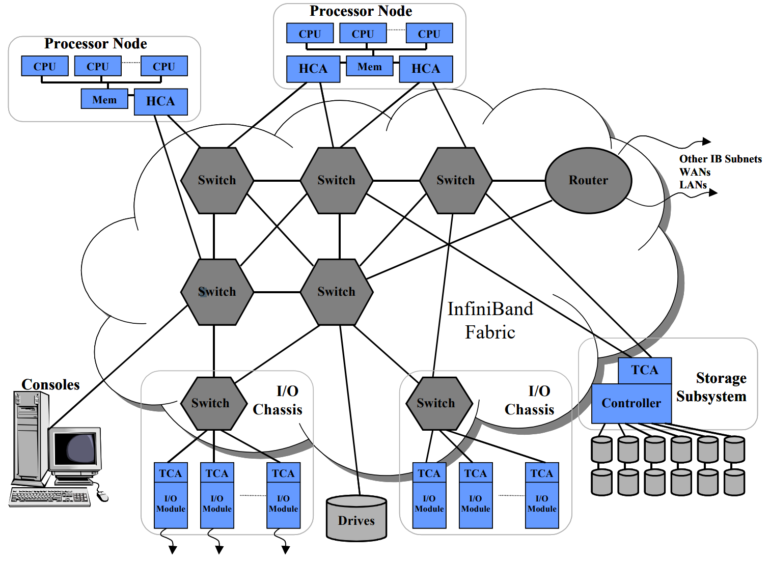
IB offers the following advantages:
- High bandwidth: 200Gb/s (MeluXina GPU, FPGA and LargeMem compute nodes have two links of this type)
- Low latency: under one microsecond for application to application
- Full CPU offload: bypass kernel and get direct access to hardware, leaving the CPU to do more computing rather than data management
- RDMA for high-throughput, low latency, and low CPU impact
- Cluster scalability: DragonFly+ topology allowing efficient connections between fabric members while maintaining high bisection bandwidth
Optimizing code executions
This section provides on overview of how to optimize code execution for the most efficient access to the MeluXina CPUs, accelerators and InfiniBand interconnect.
In shared-memory parallelism, pinning a thread to a specific compute resource (at the level of a node, socket or core) refers to the advanced control of thread allocation, while binding refers to the advanced control of process allocation in distributed-memory parallelism. Binding and pinning are very important for best application performance, enabling applications to avoid useless remote memory access when possible and increasing local memory access (data locality).
Note
Pinning and thread affinity are interchangeable as well as binding process and process affinity.
Default binding/pinning strategy on MeluXina
It is important to be aware of the pinning/binding settings of the CPUs to the interconnect in order to optimize performance. The binding setting of MeluXina nodes are described in the table below:
| Compute node | NUMA options |
|---|---|
| CPU | NPS=4, 8 NUMA domains and 2 sockets per node NUMA node 0 and 3 attached to HCA Default CpuMap |
| GPU | NPS=2, 4 NUMA domains, 2 sockets per node and 1 NUMA domain per GPU 2 NUMA nodes attached to HCAs CpuMap modified to prioritize NUMA nodes with HCA |
| FPGA | NPS=4, 8 NUMA domains, and 2 sockets per node Default CpuMap |
| Large memory | NPS=4, 8 NUMA domains NUMA node 0 attached to HCA CpuMap modified to prioritize NUMA nodes with HCA |
| NPS=NUMA Per Socket HCA=Host Channel Adapter |
As of October 2021, for all compute nodes the default binding/pinning behavior is as follows:
- Tasks/processes are not pinned/bound to memory as
SLURM_MEM_BIND_TYPE,MEMBIND_DEFAULTor--mem-bind=are set tonone. However, any task/process from any CPU can use any (remote) memory.
SLURM_MEM_BIND_TYPE=none
- For binding tasks/processes to CPUs, set
threads(throughSLURM_CPU_BINDor--cpu-bind) to automatically generate masks binding tasks/processes to the threads. The distribution of tasks/processes to the nodes on which resources have been allocated, and the distribution of those resources to tasks for binding (task affinity) is set toblock. The block distribution method will distribute tasks to a node such that consecutive tasks share a node. This minimises the number of nodes/sockets required in order to prevent fragmented allocation.
 SLURM_CPU_BIND=threads
 SLURM_DISTRIBUTION=block
Note
The first Slurm distribution level is not relevant for task binding inside a compute node as it governs the distribution of tasks across nodes.
-
For binding tasks/processes to sockets (NUMA nodes on MeluXina) is set to
cyclic. The cyclic option is used as second distribution method forSLURM_DISTRIBUTIONor--distributionvariables. The cyclic distribution method will distribute tasks to a socket such that consecutive tasks are distributed over consecutive sockets (in a round-robin fashion).- On CPU nodes, tasks pinning/binding prioritize NUMA node 0 and 3 which have HCA attached.
- On GPU nodes, each task is assigned a GPU belonging to the NUMA node of the CPU the task is assigned to.
- On Large memory nodes, tasks pinning/binding prioritize NUMA node 7 which has HCA attached.
-
The third distribution level, pinning/binding tasks/processes to CPU cores is set to
inherit(inherited from second distribution method =cyclic).
Warning
A socket is actually a NUMA domain in our current slurm configuration.